Heat/Light Activated Switch - SCOPES Digital Fabrication

Lesson Details

Age Ranges
Standards
Fab-Safety.1, Fab-Electronics.1, Fab-Modeling.1, Fab-Fabrication.1, Fab-Design.1, Fab-Safety.2, Fab-Electronics.2, Fab-Modeling.2, Fab-Fabrication.2, Fab-Design.2, Fab-Safety.3, Fab-Electronics.3, Fab-Fabrication.3, Fab-Design.3

You need to login or register to bookmark/favorite this content.

Author

Brandon Prentice
Brandon Prentice
K-12 teacher
Brandon Prentice is a fabrication teacher and instructional coach for the Trinity-Area School District, located in southwestern Pennsylvania.  He is a graduate of California University of Pennsylvania, earning his BS and MEd in Technology Education. A major part of his… Read More

Summary

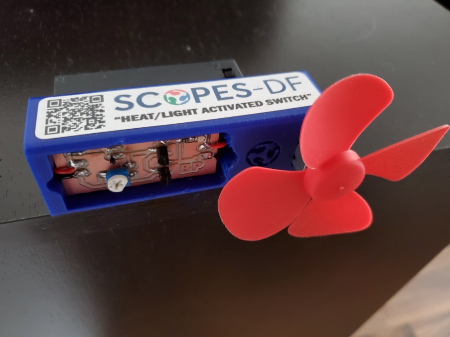
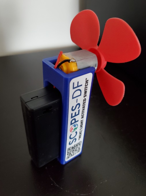
The purpose for this lesson is to teach grades 11-12 students the concepts of transistors, while also introducing electronics design software to digitally fabricate a transistor switch circuit. The challenge is to design a temperature activated switch that can also act as light activated by swapping one sensor. The output of this board can be used to control other electronic circuits, turning them on automatically either when it goes hot/cold or light/dark. High school students design this project to learn electrical engineering concepts such as; schematic/board layouts, soldering techniques, operating transistors, and the fabrication of circuits. Students have the option to go an extra step further by digitally fabricating their own circuit enclosure and designing their own marketing labels.

What You'll Need

TOOLS/MACHINES


  • CNC high precision milling machine
  • Soldering iron(s)
  • Wire strippers, pliers, tweezers, etc.


SOFTWARE


  • Electronic Design (KiCad or Similar)
  • CNC Mill CAM Software (Fab Modules or Similar)


MATERIALS


  • 2″x3″ Blank Copper PCBs
  • (x1) 2 AA Battery Pack (3V total)
  • (x1) 3-6V DC Motor (2mm shaft)
  • (x1) Plastic Fan that fits 2mm shaft DC Motor
  • (x1) 47K Potentiometer
  • (x2) NPN Transistors
  • (x1) Thermistor OR (x1) Photocell
  • (x2) SMD 220 ohm Resistors
  • (x1) SMD LED


The Instructions

Understanding Transistors/Darlington Pair

Students learn the basics when it comes to regulating voltages and understanding transistors. Using transistors in a Darlington Pair is the heart of this project so in order to create the circuit students must first learn all of the components involved.

Before getting into the fabrication and design aspect of the switch, it is important to first explain to students why they are using transistors and what importance they have in the digital age.


Image result for transistors


Image result for darlington pair


Here is an example video of some simple explanations of a transistor: https://www.youtube.com/watch?v=7ukDKVHnac4


Some important factors to address when it comes to using transistors as a switch circuit:


  • Understand what an Transistor is and how it works
  • Differences between NPN and PNP
  • Using the Darlington Pair
  • What is current gain
  • Relationships to logic gates and modern day computers


Electronics Design (KiCad)

Students will be introduced to the basics of Electronics Design using the KiCad software. All footprints for the components used are under Attachments as a .Zip file. This folder can be sync directly to KiCad for access.

Image result for kicad logo


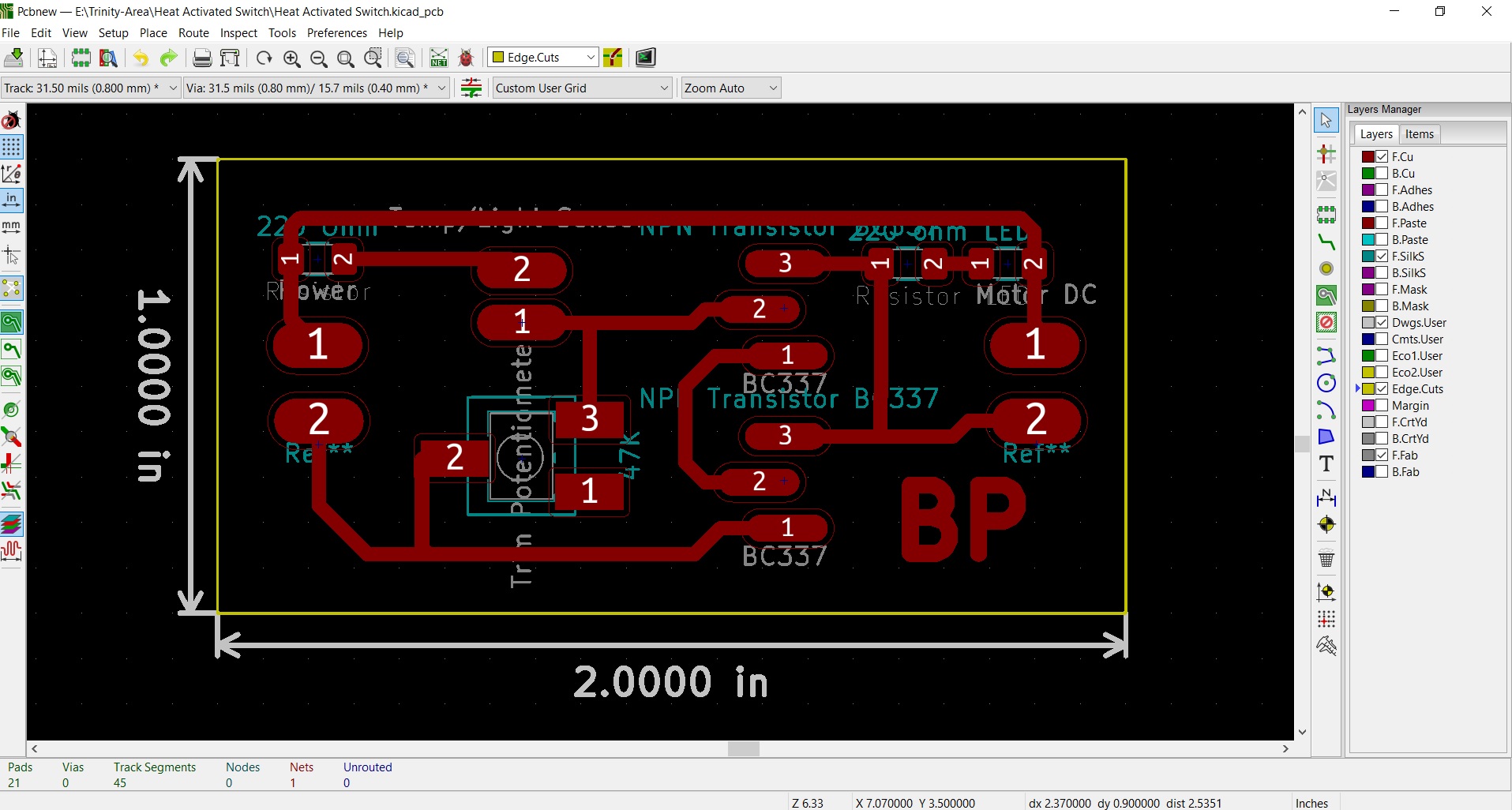
This portion of the lesson must be taken slowly for high school students if the class has not yet been exposed to circuit design. The goal is for students to take an existing schematic and create their own board design that is 2″ x 1″ in size. Here are the two different schematics to choose how the switch performs:


Break down all of the essential features and tools of a design software (KiCad, Eagle, Etc.) in order to guide students in the following:


  • Schematic Captures
  • PCB Layouts
  • Fabrication Design Rules
  • Component Placement
  • References/Labeling
  • Graphic Lines
  • Board Dimensions/Measuring
  • Text Tool
  • Netlists
  • Ratsnest
  • Routeing
  • Layers Manager
  • Export Settings into Black/White SVG File


Electronics Production (CNC Milling & Soldering)

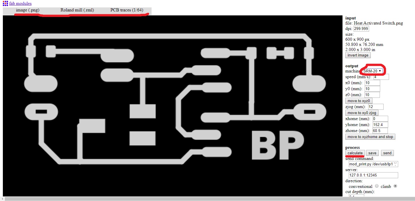
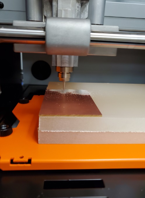
Students learn the next fabrication process by taking their finished circuit design into a milling machine. By taking an exported (Black/White) SVG file, they can then utilize the Fab Modules toolpathing software (www.fabmodules.org) to produce a circuit board.

The fab modules provide a set of software tools for personal fabrication, intended for use with machines common to fab labs. It Functions to generate 2D and 3D toolpaths for our circuit production and runs off any web browser from www.fabmodules.org. Once students are on the website, they first input the correct .SVG file they created earlier while also pressing “invert image” to get the correct contrast.


Once inverted, they must select the appropriate output file depending on the CNC Mill being used, and finally make sure that the toolpath is intended for “PCB Traces (1/64)”. See Below:


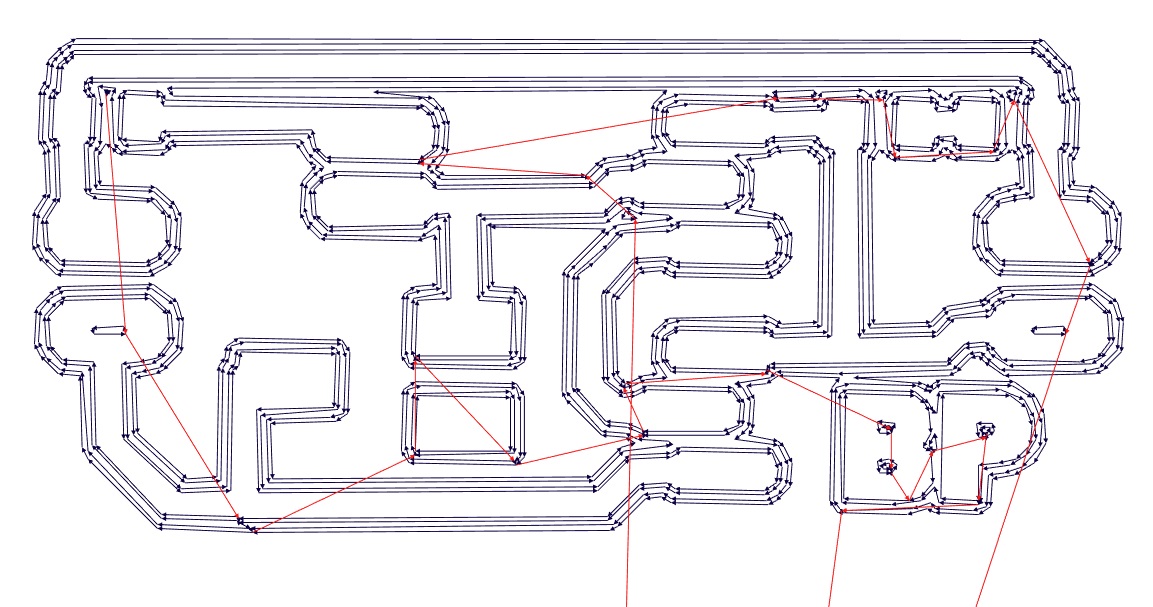
At the end they must hit “calculate” in order to generate the toolpath and then click “save” to make a G-Code specific to the previously chosen machine.


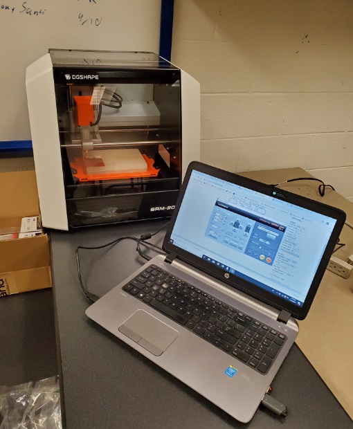
All CNC machine operations is then done at the instructor’s or manager’s expense and is specific to every Fab Lab.


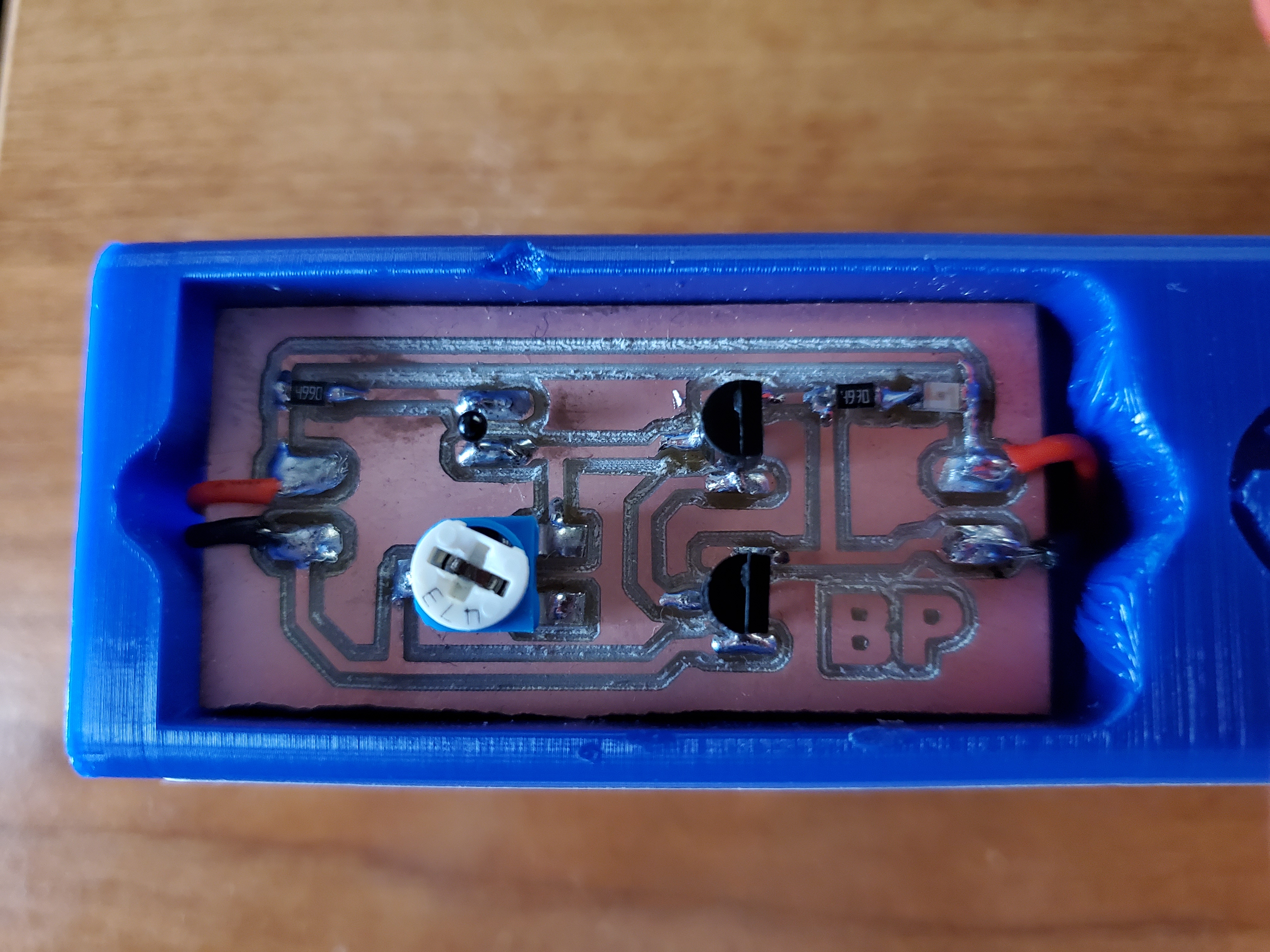
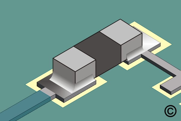
Soldering All Surface Mount Devices (SMD) & Wires:


Solder the following components onto the appropriate pads based off the schematic design:

  • +&- Wires of Battery Pack
  • +&- Wires of DC Motor
  • [x2] 220 ohm SMD Resisters
  • [x1] SMD LED
  • [x2] Transistors
  • [x1] 47k Potentiometer
  • [x1] Thermistor OR Photocell


Related image

Related image


(Optional) 3D Printed Casing with Vinyl Printed Labeling

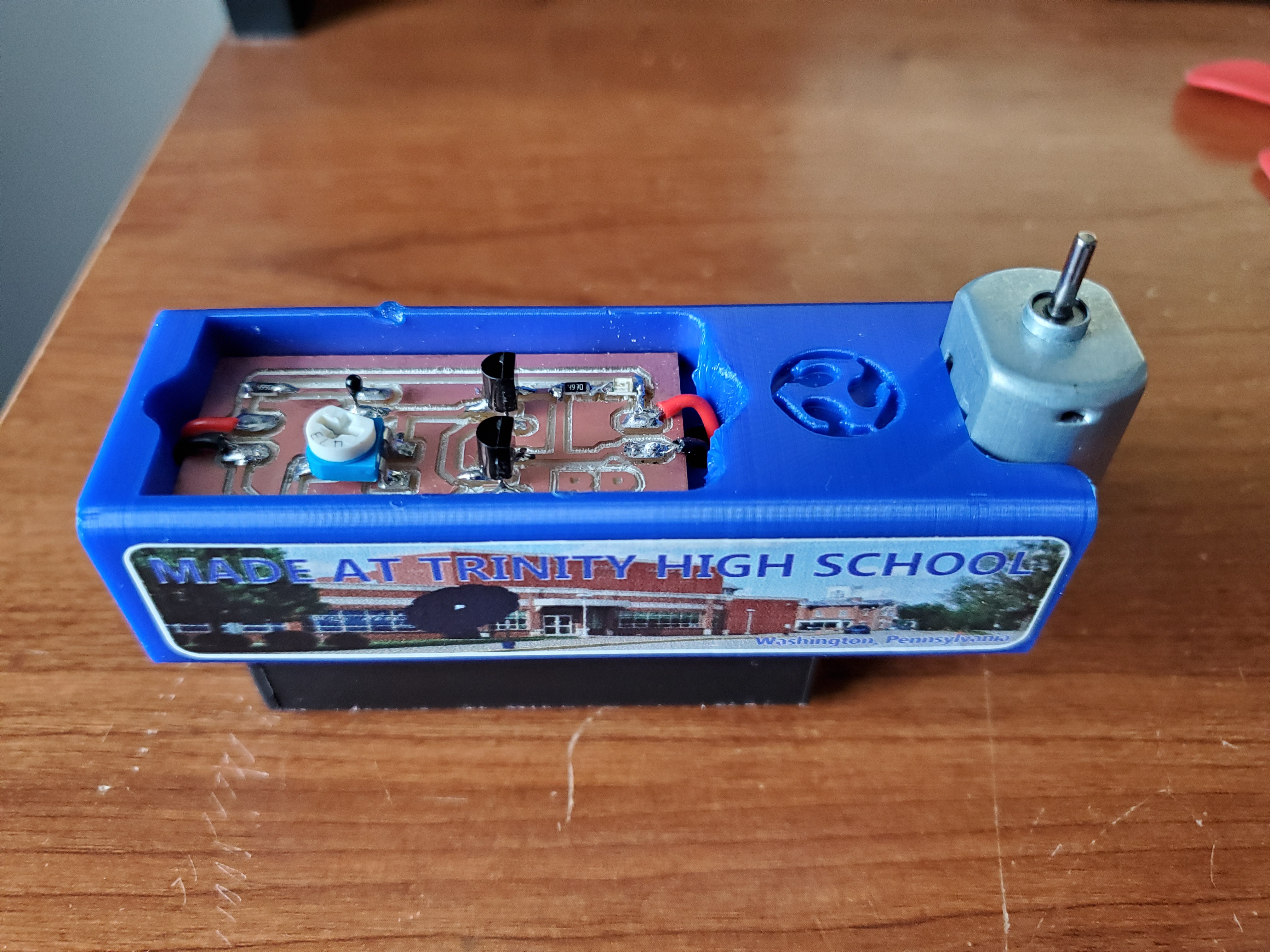
Students can either design their own 3D printed casing or produce the existing that I've attached to this lesson. Students can also design any custom labels from a vinyl printer/cutter onto their casings.


Standards

  • (Fab-Safety.1): I can safely conduct myself in a Fab Lab and observe operations under instructor guidance.
  • (Fab-Electronics.1): I can follow instructions to build a simple electrical circuit using conductive material, basic components, and power.
  • (Fab-Modeling.1): I can arrange and manipulate simple geometric elements, 2D shapes, and 3D solids using a variety of technologies.
  • (Fab-Fabrication.1): I can follow instructor guided steps that link a software to a machine to produce a simple physical artifact.
  • (Fab-Design.1): I can be responsible for various activities throughout a design process within a group under instructor guidance.
  • (Fab-Safety.2): I can operate equipment in a Fab Lab following safety protocols.
  • (Fab-Electronics.2): I can follow a schematic diagram and create a circuit including a microcontroller with electronic components.
  • (Fab-Modeling.2): I can construct compound shapes and multi-part components ready for physical production using multiple representations.
  • (Fab-Fabrication.2): I can develop workflows across four or more of the following: modeling softwares, programming environments, fabrication machines, electronic components, material choices, or assembly operations.
  • (Fab-Design.2): I can participate in design reviews with prepared presentation materials as well as give and receive feedback from peers.
  • (Fab-Safety.3): I can supervise others in a Fab Lab and ensure safety protocols are being followed.
  • (Fab-Electronics.3): I can create my own schematic diagrams and use them to build electronic circuits including microcontrollers.
  • (Fab-Fabrication.3): I can make my own applications, electronic components, or machines to solve new problems and to grow my Fab Lab's capacity.
  • (Fab-Design.3): I can initiate design processes to generate multiple solutions to problems I have framed for multiple stakeholders.

Lesson Feedback